
PCB Design Tutorials
by David Kohanbash on January 2, 2014
Hi all
I got a question about PCB design for robots. I am not going to recreate what is already out there so here are some links.
UPDATE: Contextual Electronics has released the entire KiCad course online. Check it out here!
The two places that I have used to get PCB’s built are:
– Advanced Circuits – A traditional fab house with lots of options and fast delivery
– OSH Park – A community PCB house. They take small orders and combine it with other people’s boards to get panels produced for a low cost. Turn around time is typically around 3 weeks for a 2 layer board, however they give 3 copies of your board for $5/sq inch.
This is a great pdf tutorial about designing PCB’s from the EEVBlog’s David L. Jones. This is about actual PCB design and not about a specific package/tool.
There are also some “advanced” topics that are harder to learn (high speed, RF, etc..). One of those is grounding. Here are a few links that might help.
– Linear Circuit Design Handbook
– Staying Well Grounded
– Partitioning and Layout of a Mixed Signal PCB
These videos are part of a larger online class that you can find at contextualelectronics.com/ about designing PCB’s with KiCad. KiCad is an opensource (free) PCB design tool.
When designing PCB’s we also want to be able to manufacture them. Here are a few videos about design for manufacturing of PCB’s.
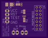
Image from http://uploads.oshpark.com/uploads/project/top_image/mKQ4o0sL/i.png

Leave a Reply